Applications Scientist Barnaby Levin giving Presentation at Spring MRS conference in Seattle Friday, April 26!

MATERIALS
TEM

Speed, Sensitivity, Versatility

Our detectors offer single electron sensitivity, fast acquisition speeds, and the ability to configure a large or small field-of-view. This allows our detectors to support a wide variety of TEM and STEM applications such as low-dose HRTEM imaging, in situ TEM, 4D STEM, and more.

Direct Detectors For Materials Transmission Electron Microscopy

Every materials transmission electron microscopy experiment is unique. Specimens can range from highly sensitive polymers, metal organic frameworks, or lithium battery materials to durable ceramic oxides or metallic nanocatalysts. The goals of a materials science experiment can vary greatly, and may include directly imaging atomic structure, measuring local chemical composition or crystal structure, or simply observing morphological changes in the specimen over time.

The diverse range of different types of materials science TEM applications can all benefit from the ability to unambiguously detect high-resolution features in an image, spectrum, or diffraction pattern. Using a poor camera that produces blurry images makes the delineation of features ambiguous, and (even worse) many high resolution features may not be detectable at all. By eliminating the scintillator, our direct detection cameras provide unprecedented resolution and sensitivity. Furthermore, the speed and range of configurations available on our detectors gives users the flexibility to optimize our detectors for a wide variety of different TEM techniques.

For a detailed description of direct detectors for materials TEM, see this article in the Journal of Physics: Materials by a member of our applications team, Dr. Barnaby Levin.

To learn more about the range of materials that researchers have imaged with our detectors, visit our Literature Library for a list of scientific publications.

Key Materials TEM Techniques

Low Dose Imaging

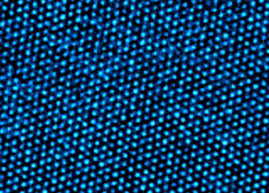
One of the key frontiers in materials science is low-dose imaging. Ideally, nearly all TEM specimens would be examined under low-dose conditions to minimize specimen damage. However, low-dose imaging has been technically challenging due to the low sensitivity of scintillator-coupled TEM cameras. Our direct detectors allow users to overcome these challenges and collect brilliant, high-resolution images even under very low dose conditions.

HRTEM Detectors:


Image acknowledgement: Gavhane et al. npj

npj 2D Materials and Applications 5, 24 (2021)

4D STEM

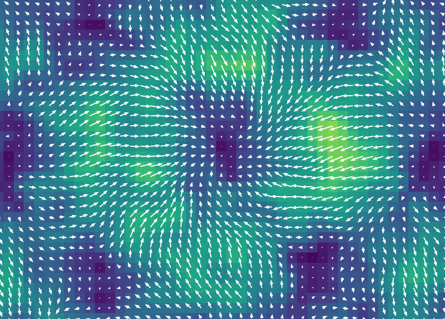
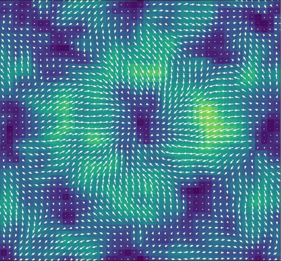
By recording complete CBED pattern at every probe position, 4D STEM allows multiple types of analyses of a specimen. These include mapping of crystal grain structure, molecular orientation, strain, and electric and magnetic fields.

Our fast, single-electron sensitive, direct detectors are ideal for rapid acquisition of high-quality 4D STEM data.

4D STEM Detectors:

 
See also our scan generator, DE-Freescan
 
Image acknowledgement: Data courtesy of Prof. Paul Voyles, University of Wisconsin Madison, USA.


In Situ TEM

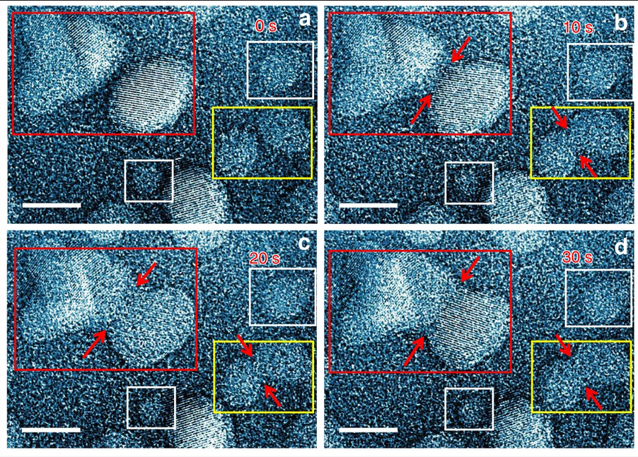
Whether observing specimens in a liquid or gas environment, or observing specimens during heating, electrical biasing, mechanical strain, or under intense irradiation, in situ TEM requires a camera with speed and sensitivity.

Our direct detectors allow you to record in situ movies with a rapid frame rate, and single electron sensitivity, so that you can get the most information possible from your specimen at a given beam dose rate.

In Situ TEM Detectors:

 
Image acknowledgement: Tian et al. Nature Communications 10 5249 (2019)

Detectors For Materials TEM

If you have questions about our products, head to our FAQ page, or contact us to learn more.

WITH GUIDANCE FROM OUR TEAM OF PH.D MICROSCOPISTS

Questions?